PCB Layout
Support various EDA tOOL layout
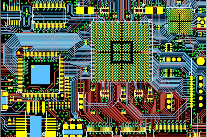
PCB Layout Design
Embizon provides complete PCB design solution to various sector/domains of the electronics industry. We are experienced in designing and detailing of 36 layer boards with high-speed SERDES and over 15,000 components. Miniature PCB design with mixed-signal design which can fit in a small tube. Our team has experience in delivering desired outputs quickly and accurately as per specifications and guidelines.
We designed complex SOM (System on Module) boards and products using various Processor like Qualcomm Q410 , Q600, Freescale, TI and other major chipsets with miniature size using HDI technology. We provide an efficient design service to our customers while taking into account all the necessary design criteria to ensure a First-Time-Right Product Design Solution. Our extensive knowledge enables the design team to deliver the product on time with cost effective solutions.